6 Adding ports
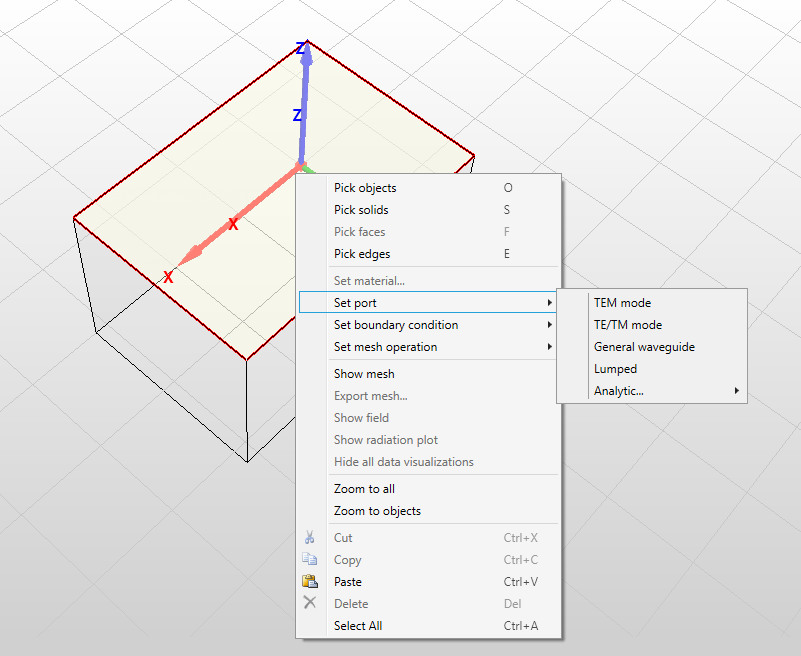
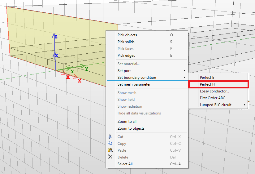
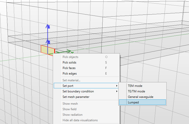
InventSim supports a few types of wave ports. Depending on the structure, you should select the port type that fits the mode type which propagates in the transmission line of a provided cross-section. To add a port to the structure, you need to select the surface that will constitute the port (to pick the surface, enable "Pick face" mode with the shortcut key "F"), then click the right mouse button and select "Set port -> ..." (Fig. 6.1) Port type cannot be changed after the port has been assigned. In order to change the type, delete the port and assign it again with a different type. To delete a port, select it in the project tree and select "Delete" from the context menu.
If the face to which a port is assigned to is deleted (either by explicit deletion or as a result of structure change), the port will be deleted automatically.
Depending on the simulation frequency, the transmission line that is defined as a port surface can guide more than one mode (there is more than one mode above cutoff). In this case, you should define the port as a multi-mode port (the option is available for a general port and TE/TM port).
The wave port can be assigned on any planar surface defined by the user, but few restrictions are enforced:
-
• The solver does not support open (radiating) transmission lines on the ports. Only closed transmission lines are supported at the moment. If a radiating boundary condition is defined at port edge, it will be neglected and transformed to a PEC on the stage of port analysis.
-
• TEM, TE/TM and general wave ports can be defined only at the outer surfaces of the domain. Lumped ports can also be defined as internal ports.
-
• The wave port should be placed at a moderate distance from any discontinuity of the transmission line. Please note that the port terminates (absorbs) only the modes that were evaluated at this port. Any other mode that propagates from discontinuity to the port will be reflected back to the structure.
-
• In general, all wave ports are normalized to the wave impedance of the line. You can re-normalize the calculated scattering parameters to characteristic impedance of the line only in the case of lumped ports.
-
• When the solver searches for modes propagating in the ports, it handles the transmission line as a lossless one. If any lossy medium is defined in the port, then the solution found by the solver might be slightly mismatched with a lossy line. An additional reflection on the connection of the lossless and lossy lines will be introduced.
-
• The port must be defined on the wall of a 3D object. Surfaces placed arbitrarily in space are not allowed.
-
• The port should enclose all the conductors needed to properly solve the excitation mode field pattern.
6.1 TEM mode ports
This type of a port can be used to simulate a homogeneous two conductor line, i.e. a coaxial line. The coaxial cable is one of the most common transmission lines used in high frequency and microwave devices. It is a two-conductor line of a cylindrical cross-section, in which an inner rod and outer shielding conductor are placed concentric on the same axis and it is usually separated with dielectric material. In this type of transmission line, the fundamental propagating mode is TEM mode with zero cutoff frequency.
In order to find the proper TEM mode template, InventSim numerically solves the Laplace equation defined by a provided port cross-section
\begin{equation} \nabla ^2 \phi = 0 \end{equation}
assuming 1V potential difference between two conductors. In this case, only a single mode propagation is available. In order to handle higher order modes, you should use a general port.
6.2 TE/TM mode port
Transverse electric (TE) and transverse magnetic (TM) are modes with non-zero cutoff that are propagating in homogeneous, single-conductor, closed transmission lines. Some examples are rectangular, circular or elliptic waveguides. To solve the TE mode template \(\textbf {E}_t\) the vector wave equation is solved:
\begin{equation} \nabla _t \times ( \mu _r^{-1} \nabla _t \times \textbf {E}_t ) - k_c^2 \epsilon _r \textbf {E}_t = 0 \end{equation}
and for TM modes:
\begin{equation} \nabla _t \times ( \epsilon _r^{-1} \nabla _t \times \textbf {H}_t ) - k_c^2 \mu _r \textbf {H}_t = 0 \end{equation}
where \(k_c\) is the cutoff frequency of the mode.
This type of a port supports multimodal regime and the number of modes is specified with cutoff frequency \(k_c\). If you introduce the non-zero cutoff frequency at the port, then the solver searches for all modes that are propagating up to a provided cutoff frequency \(f_c\). Please note that you will get a multimodal (generalized) scattering matrix as the simulation result.
Efficiency notice: TE/TM ports are solved using a dense matrix eigensolver, which can be computationally intensive for very dense meshes at the ports. In this case, it is recommended to use general ports that use sparse matrix computations.
6.2.1 Degenerate TE/TM modes
In some, special transmission lines, (i.e. circular or square waveguide) a pair of modes with the same cutoff can propagate along the line with the same propagation constant, but different polarization. It is very difficult to properly control the polarization of both numerical solutions unless the analytic solutions are known and used. At the moment, InventSim might produce inaccurate results for ports with degenerate mode propagation. One can overcome this by slightly changing the cross-section. As an example: instead of square waveguide with sidewall dimension \(a=20mm\), simulate rectangular waveguide with dimensions \(a=20mm\) and \(b=20.01mm\).
6.3 General ports
This type of a port is the most robust one and it can be applied to transmission lines with any cross-section, including waveguides loaded with inhomogeneous dielectrics. The most common application of this port would be a microstrip line, a co-planar waveguide or a partially filled rectangular waveguide. To solve the mode template at the port, a three-component vector field formulation is implemented, which solves the equations:
\begin{equation} \textbf {E} = \textbf {E}_t + \hat {n} E_z \end{equation}
\begin{equation} \nabla _t \times ( \mu _r^{-1} \nabla _t \times \textbf {E}_t ) - \mu _r^{-1}(j \beta \nabla _t E_z - \beta ^2 \textbf {E}_t) = k_0^2 \epsilon _r \textbf {E}_t \end{equation}
\begin{equation} -\mu _r^{-1} [ \nabla _t \cdot ( \nabla _t E_z + j \beta \textbf {E}_t ) ] = k_0^2 \epsilon _r E_z \end{equation}
for a provided frequency \(k_0\).
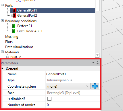
General ports can also handle multi-modal propagation. In port options, you can specify the number of modes that should be taken into account during the simulation (Fig. 6.2). Initial value equal to zero means that just a fundamental (lowest cutoff) mode is found. For example, if you simulate coupled microstrip lines that consist of three conductors, then two modes should be defined at the port.
You can also add a coordinate system to the port with (
 ) icon. If one is added, the solver will try to align the sign of the electric field component of mode template with Z-axis of coordinate system defined at the port.
In these types of ports, a mode template has to be found on each frequency and the associated numerical cost is the highest when compared to TEM or TE/TM modes. In that respect, the TEM ports or TE/TM ports should be used, if possible, to reduce the computational cost involved.
6.3.1 Microstrip and CPW ports
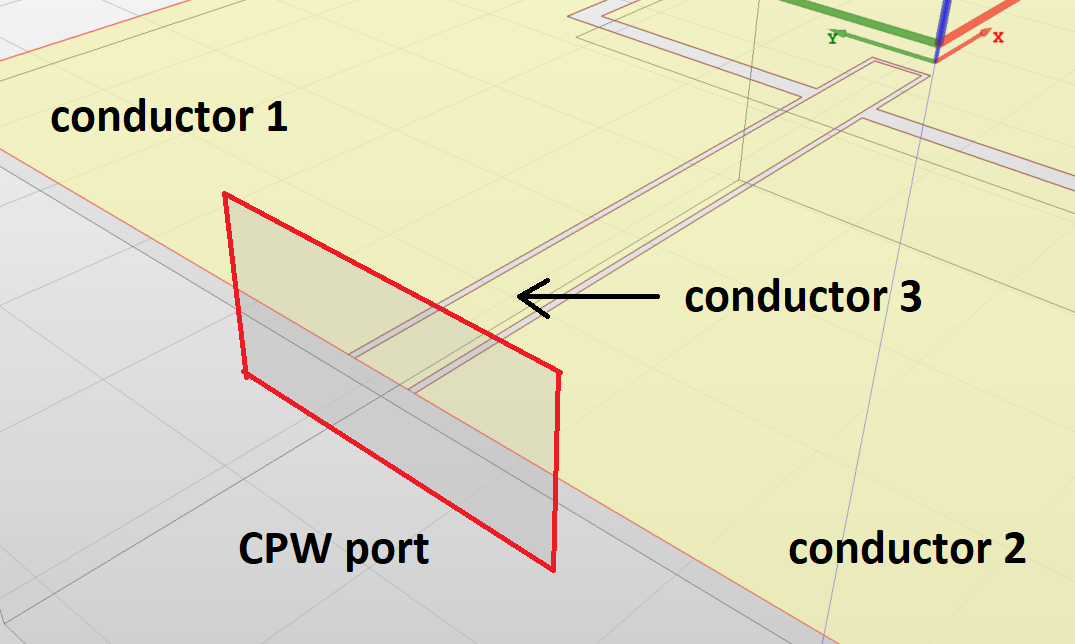
Both CPW and microstrip lines are in, general, in-homogeneous cross-section lines. To properly simulate the devices with those line types, general ports should be used. Additionally, since the CPW line is a three conductor line, it guides two different modes with zero cutoff frequency (even and odd) (Fig.6.3). In order to properly solve the CPW line, both modes should be taken into account during the simulation by setting the number of modes in the port as two. Then you can identify the mode you are mainly interested in (usually the even mode).
6.4 Lumped ports
Lumped ports are the only ports that can be placed inside of the domain and assume that the port is much smaller compared to the wavelength. The surface on which the port is defined must cover at least two conductors. To define a lumped port, you need to also define a voltage plan - i.e. assign voltage (0V or 1V) for each conductor. Then, during the simulation, the solver computes the currents that flow between the conductors and calculates the impedance parameters.
Please note that in InventSim lumped ports should be defined on homogeneous dielectric areas!
6.4.1 Adding lumped ports
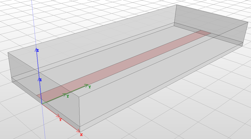
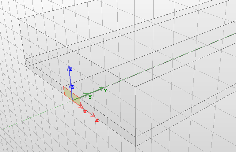
To show an example of the lumped port definition, let us look at the microstrip line structure shown in Fig. 6.4. The structure consists of two box objects representing the dielectric substrate layer and the air above it. It also consists of a 2D rectangular object that is a PEC strip. To excite the structure with lumped ports, you need to define the port area first. In this case, it is a small rectangular area between the strip and the ground-plane.
Draw a 2D rectangle that covers this area, as shown in Fig. 6.5. Then modify the default boundary condition on the wall from PEC to PMC (otherwise the strip would be shorted to the ground, Fig. 6.6. In the next step, select the 2D rectangle object and select "Set port -> Lumped" (Fig. 6.7 from the context menu.
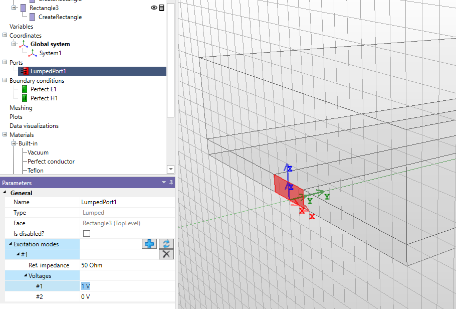
A new lumped port will be added. Select this port, go to the properties window and add an excitation mode template (using
icon). InventSim will process the port area to find the conductors defined at the port. Once that is done, the conductors will be shown in the 3D view and marked with labels (Fig. 6.8). With the voltage plan options, you can define the value of voltage for each conductor - in this case it is 0V for the ground-plane and 1V for the conducting strip.
Optionally, you can define the reference impedance (default is 50 Ohm) used to re-normalize calculated scattering parameters.
The user can optionally apply port calibration, i.e. technique that removes the port discontinuity from the numerical simulations. This might influence the simulation results in high frequency regime.
To properly model lumped ports (defined on 2D objects), InventSim requires them to be drawn on the surfaces or walls associated with 3D objects. If the lumped port is drawn inside of the volume, an auxiliary 3D element should be drawn and the port should be defined on the surface of this 3D object.
6.5 Analytic ports
Analytic ports provide a way to specify the excitation within the port plane using analytical solutions for modes propagating in strictly rectangular or circular waveguides. This capability enables precise control over the excitation’s phase and ensures accurate computation of the resulting scattering parameters.
Important Note: When dealing with square waveguide or circular waveguide ports, it’s crucial to understand that numerical solutions for mode field templates cannot offer exact mode polarization definitions.
-
• In the case of square waveguides, the numerical solution describes a linear combination of the \(TE_{10}\) and \(TE_{01}\) modes.
-
• or circular waveguides, the degenerate solutions for \(TE_{mn}\) or \(TM_{mn}\) waveguide modes with \(m \ne 0\) are indistinguishable in the solution.
Only the use of analytic field templates allows the user to properly define excitation in this scenario, and we strongly recommend employing analytic modal field solutions.
To define an analytic mode template, the user must provide additional information regarding the mode type (TE/TM) and the mode indices (m, n). Modes can be added with port’s property panel. The modes align with the local coordinate system defined at the port, with the "z" direction indicating the propagation direction. User can add more than one mode to the port, enabling the calculation of multimodal, generalized scattering matrix of the component.