2 Quckstart: Simulation of a microstrip stub
Let us begin with the task of simulating a electromagnetic field and a transfer function for a device that consists of a stub that is connected in parallel to planar transmission line printed on the dielectric layer. This type of structure is called a microstrip line with a stub in microwave engineering.
In most cases, the electromagnetic field simulation of any device (or circuit) with InventSim would consist of three basic steps:
-
1. Definition of geometry of the structure, materials and the boundary conditions,
-
2. Setting the simulation options (meshing, frequency plan, solution technique),
-
3. Visualization of simulation results (electromagnetic field distribution and/or transfer function).
2.1 Construction of a 3D model
To create a 3D model:
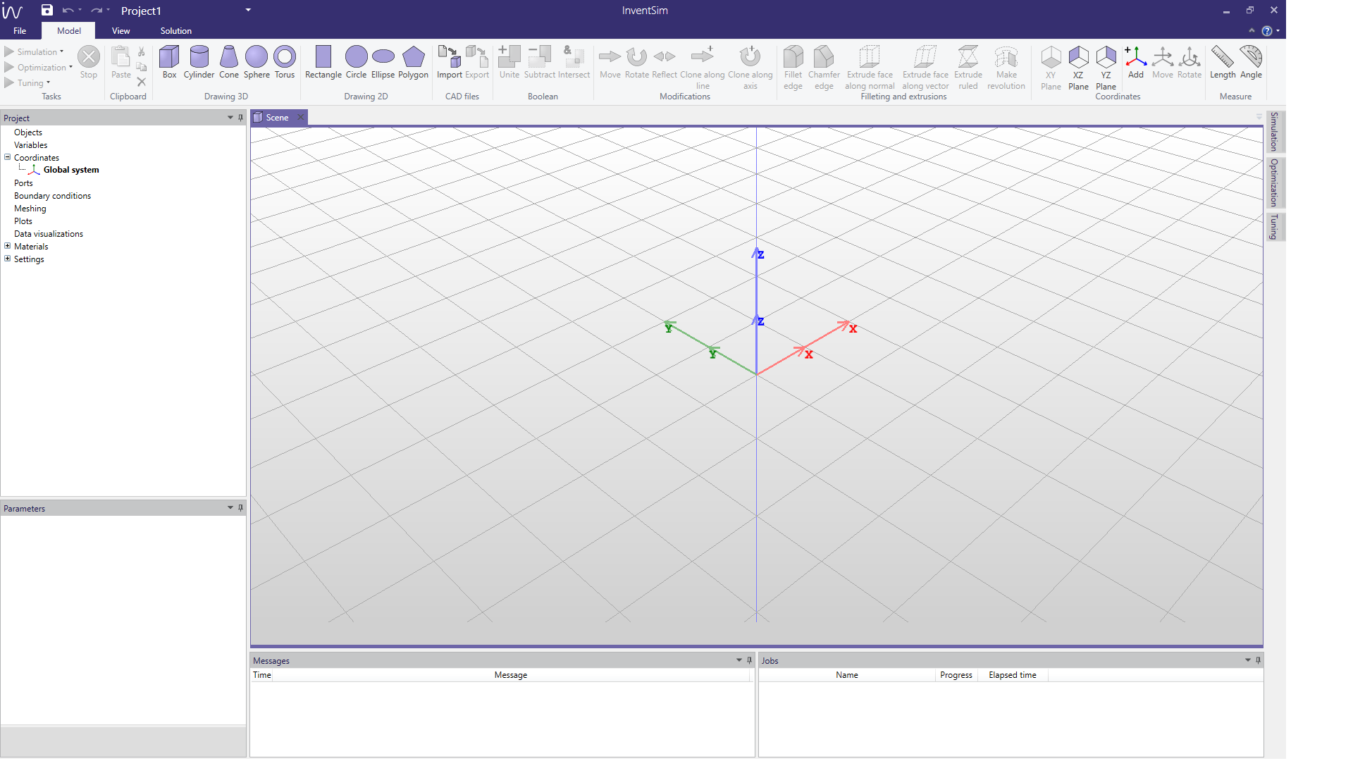
Launch InventSim and add a new, empty project. You should see a window shown in Fig 2.1:
-
• The toolbar with icons that allow you to create and manipulate objects - located on the top of the window.
-
• The tree of objects, coordinate systems, boundary conditions, field and mesh visualizations etc. located on the left.
-
• Tabs with simulation and optimization settings hidden on the right (auto-hide mode is enabled by default).
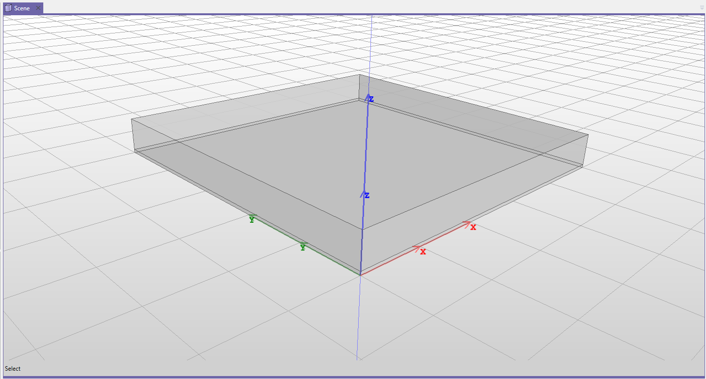
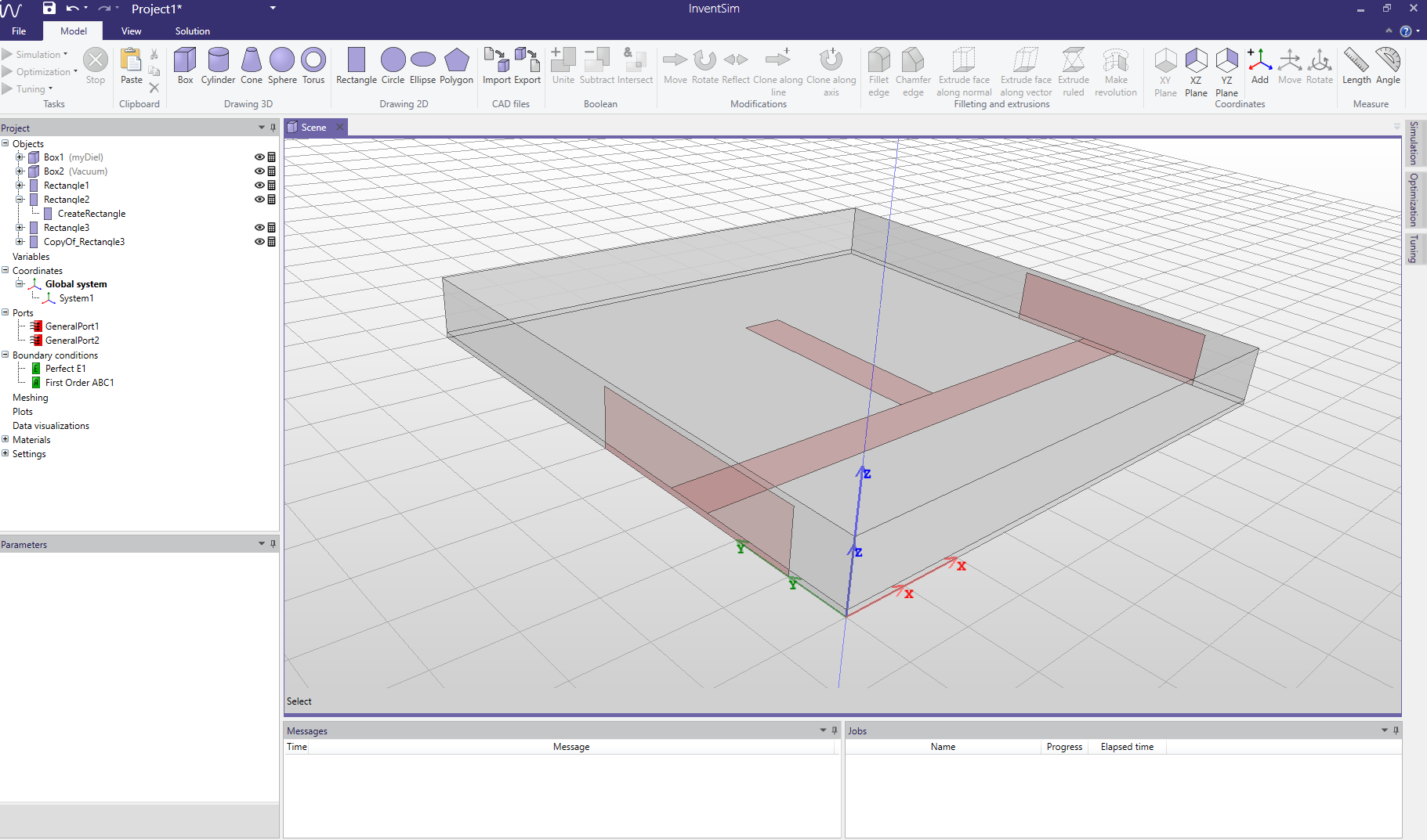
In order to define the structure we need to draw two boxes - one for the dielectric substrate and the second to model the air (vacuum) above the substrate. To start, click the box icon (
![]() ). Draw one box starting from point (0,0,0) with dimensions XDim=50, YDim=50, ZDim=0.508 - please note that the default length unit is a millimeter (mm). Draw the second box, starting from point (0,0,0.508) with
dimensions XDim=50, YDim=50, ZDim=5. The result should be as it is in Fig 2.2. Please note that the default boundary condition enforced on
the outer surfaces of our model is always that of a perfect conductor (PEC). In result, at this point both vacuum boxes are surrounded by perfectly-conducting metallic walls. The lower surface of box representing the
dielectric layer is therefore a PEC surface and constitutes a groundplane of a microstrip line.
). Draw one box starting from point (0,0,0) with dimensions XDim=50, YDim=50, ZDim=0.508 - please note that the default length unit is a millimeter (mm). Draw the second box, starting from point (0,0,0.508) with
dimensions XDim=50, YDim=50, ZDim=5. The result should be as it is in Fig 2.2. Please note that the default boundary condition enforced on
the outer surfaces of our model is always that of a perfect conductor (PEC). In result, at this point both vacuum boxes are surrounded by perfectly-conducting metallic walls. The lower surface of box representing the
dielectric layer is therefore a PEC surface and constitutes a groundplane of a microstrip line.
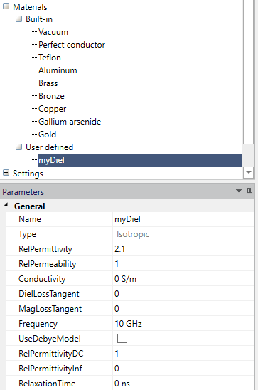
At this point, we should have two objects on the objects list (located on the left): both made of vacuum. Let us add a new dielectric material with dielectric relative permittivity equal to \(\epsilon _r=2.1\). Click the "Materials" from the project tree, click the right mouse button and select "Add->Isotropic". You can find a new position "Material1" on the list of materials. This position can be edited. Rename the position to "myDiel" and enter the relative permittivity to "2.1" as shown in Fig. 2.3. At this point, you can also change the appearance of the objects made from this material (for example, color and transparency).
Once you have added the material, you can assign it to the box representing the dielectric layer. Select the box from the objects list, click the right mouse button, select "Set material..." from the context menu and select "myDiel" from the list of available materials.
At this point you have defined a basic 3D object. The next step is to define the microstrip transmission line that will be represented as a 2D object - the rectangle located on the top of dielectric layer.
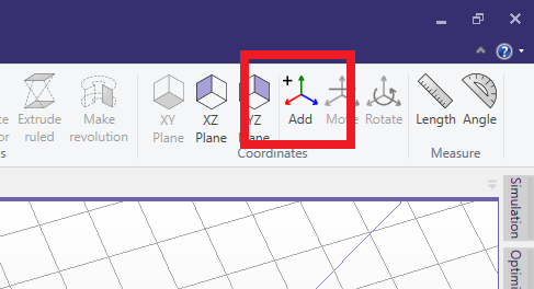
In InventSim, 2D objects are always placed on the XY, XZ or YZ planes of the current coordinate system. If you want to put a metallic strip on the upper layer of the dielectric, you need to introduce a new coordinate system that will
lay on the upper surface of the dielectric. Click the "Add coordinate system" icon from the upper toolbar (
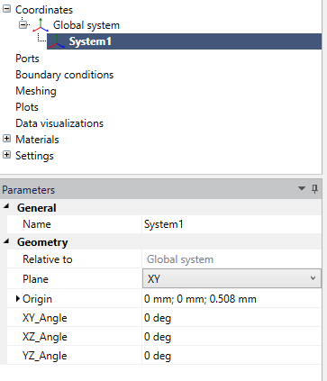
![]() , Fig.2.4) and put it in location X=0, Y=0, Z=0.508 (Fig.2.5).
, Fig.2.4) and put it in location X=0, Y=0, Z=0.508 (Fig.2.5).
This new coordinate system becomes active and you are ready to draw 2D objects on top of the dielectric (plane XY in newly added coordinate system).
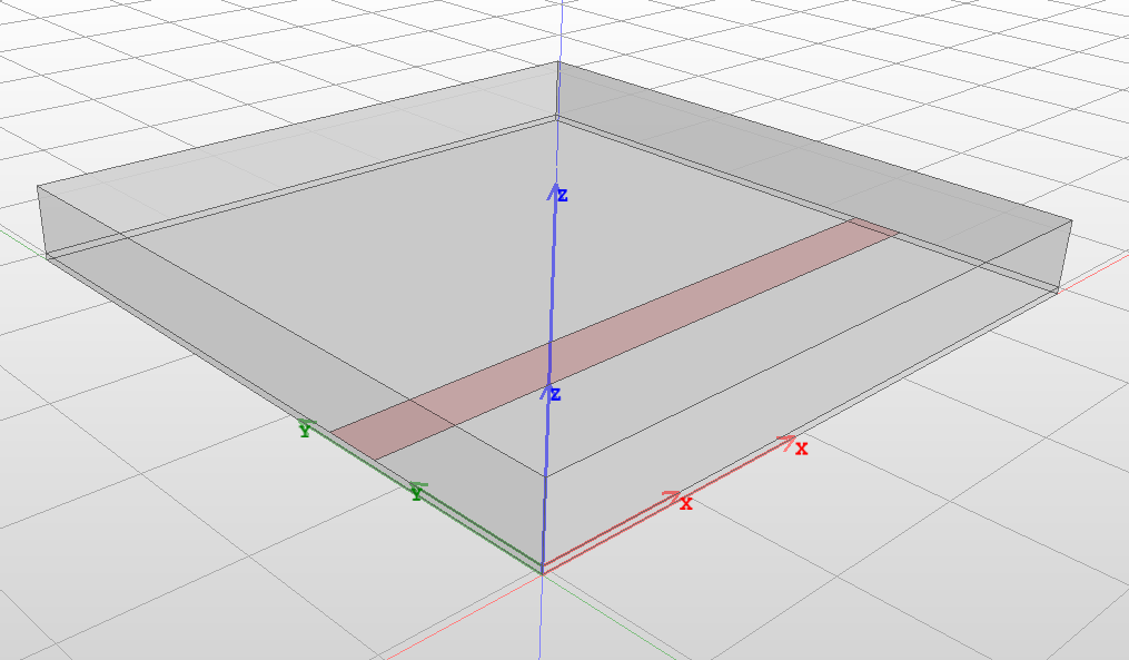
Draw a rectangle starting from point X=0, Y=13 and size it XDim=50, YDim=4 using the draw rectangle icon (
![]() ). The result is shown in Fig. 2.6. Add a section of transmission line connected in parallel to the first one (right in the middle). Draw a second
rectangle starting from point X=23, Y=17 and size it XDim=4, YDim=20. When entering the "YDim" you can also define it as a variable by entering "L=20". In that case, the variable named "L" would be added to a variables list and
initialized with value 20.
). The result is shown in Fig. 2.6. Add a section of transmission line connected in parallel to the first one (right in the middle). Draw a second
rectangle starting from point X=23, Y=17 and size it XDim=4, YDim=20. When entering the "YDim" you can also define it as a variable by entering "L=20". In that case, the variable named "L" would be added to a variables list and
initialized with value 20.
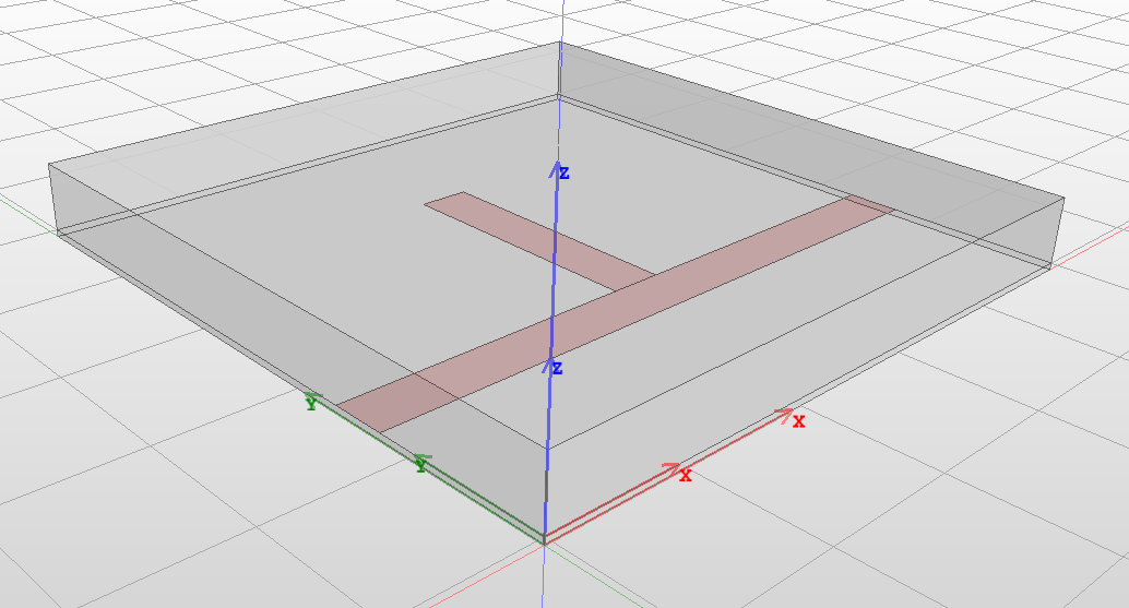
The final model of the structure is shown in Fig. 2.7.
When looking at the list of objects, it is visible that both 2D objects (rectangles) do not have any materials assigned to them. In InventSim, 2D objects do not have definable material properties like the 3D objects. Instead, you can only define boundary conditions enforced on their surface. In this case, in order to make them metallic strips, you need to select each of them, click the right mouse button and select "Set boundary condition-> Perfect E". This enforces the surface to be a perfect electric conductor. You can notice that after doing this, new elements are shown on the project tree list in the "Boundary conditions" category.
The next step is to define an excitation for our structure - in this case, it will be two wave ports on both ends of the microstrip transmission line. Draw two rectangles representing ports on the YZ plane - it is possible to select this plane using the "YZ Plane" icon from the upper toolbar. Afterwards, switch back to the global coordinate system by selecting it from the list of coordinate systems on the project tree and clicking "Activate". Now, you can draw a rectangle starting with point Y=5, Z=0 and size it YDim=20, ZDim=5. This object ("Rectangle3") will be the first port.
You can select this object from the objects tree and copy and paste it using the Ctrl+C, Ctrl+V keys. A new object named "Copy of Rectangle 3" appears, which can be moved to the opposite surface of the domain by using the "Move" operation with offset X=50, Y=0 and Z=0. Finally, select "Rectangle3", click it with the right mouse button, select "Set Port -> General Waveguide". Do the same for the other port.
You can also make the structure open from the top: select the upper surface of the object representing the air/vacuum and therefore enforcing absorbing boundary condition on it (click the right mouse button on the object, select "Pick Faces", then pick the face of the object, use the right mouse button on the object again and select "Set boundary condition -> First order absorbing").
After going through all the steps described above you should see the same structure as the one in Fig. 2.8.
2.2 Simulation setup
Once the structure geometry, materials and boundary conditions are defined, let us can move on to the simulation setup. On the right of the main InventSim window, locate the "Simulation" tab. The tab allows you to define the settings for meshing and a frequency plan.
When it comes to the mesh, you can simply restrict the maximum mesh size to not be greater then the provided value - in this case, define it as 2mm, as shown in Fig. 2.9. More advanced meshing options are described in chapter 7 1
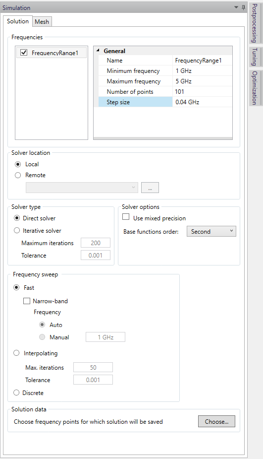
The next step is to define the frequency plan. Add one by clicking the right mouse button on the "Frequencies" box (it should be empty at this point) and select "Add". Then, assign a frequency plan: the starting frequency (1GHz), stopping frequency (5GHz) and the number of frequency points (101), as shown in Fig. 2.10.
In the lower part of the window, you can find a set of options for a fast frequency sweep. Enable this in this project and select the "Wideband" option. More on this setting can be found in chapter 8.
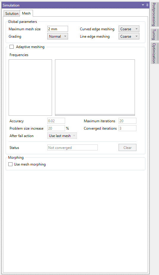
1 Please note that proper meshing is crucial for the quality of your solution and the accuracy of simulation results. In this Userguide, we perform a coarse simulation of our structure.
2.3 Simulation and postprocessing
The model is now ready for simulation. It is recommended to save the project on your hard drive before starting the simulation.
Once that is done, click the simulation icon on the upper left toolbar (
![]() ). The simulation will then start and the progress will be displayed on the "Messages" and "Jobs" windows at the bottom of the main InventSim window. The simulation starts with the processing of geometry, followed by the
mesh generation and the problem solution (which is usually the most computationally intensive part).
). The simulation will then start and the progress will be displayed on the "Messages" and "Jobs" windows at the bottom of the main InventSim window. The simulation starts with the processing of geometry, followed by the
mesh generation and the problem solution (which is usually the most computationally intensive part).
Once the mesh is ready, it can be displayed with the right mouse click on the 3D view window and selecting "Show mesh".
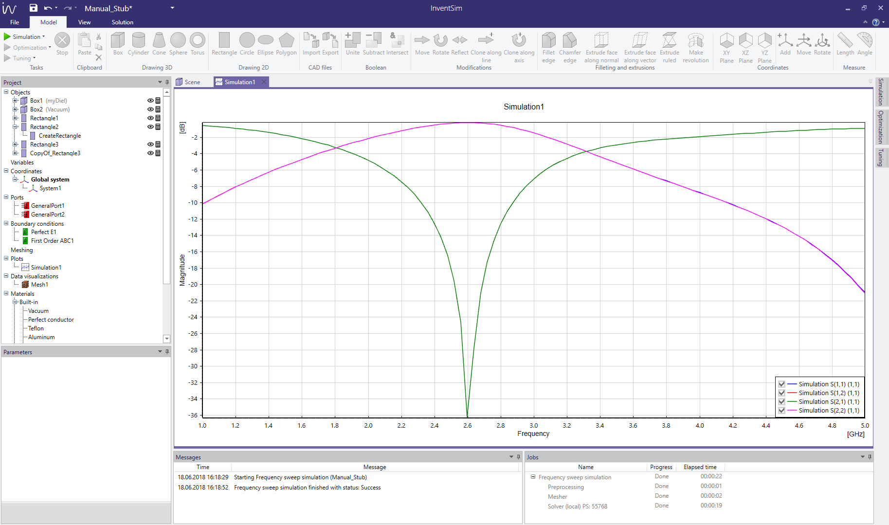
After simulating, you may add a plot of circuit response (usually, scattering parameters). Click the "Solution" tab on the upper toolbar and select "Add rectangular" to define a new plot and select data series displayed (see section 9.1) for details). You can zoom in on the plot, add markers or modify the dataseries by using the context menu with the right mouse click on the plot.